
- Company overview The heart of SMC Vision & Philsophy Partnership Certifications Company culture
- Our service Design and Engineering Maintenance and Service Examine Production Line Upgrade and Transformation Storage and Logistics Processing, Trading and Distributor
- Management Our history Global responsibility Info Center
- Procurement center Internship
- Construction & Real Estate
- General Mechanical Equipment Refrigeration Equipment Metal & Metallurgy Machinery Other Equipments Compressor
- Safety Roadway Safety Personal Protective Equipment
- Mechanical Basic Parts Bearing Spare Parts
- Hardware Tools
- Instrumentation Testing and Analysis Instruments Other Instrumentations
- Electrical & Electronics
- Construction Machinery Lifting Machinery Earth Moving machinery Road Construction Machinery Drilling Machinery Logistics Machinery Generator Set & Engine Other Machinery
- Rubber & Plastics Plastic Pipes and Pipe Fittings Fiberglass Reinforced Plastic Pontoon System PCTFE Product Polymer Material
- Industrial Gas Container
- Hotel Equipment & Supplies
- Daily Necessities Fabric Products Glasswork Pet Supplies
- Environmental Protection Machinery
MEMS Sensor IC Package Substrate


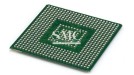
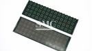
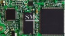


Grade: R-1566、R-357AD
Size: 100μm~130μm
Pad pitch: 0.4 mm, 0.5 mm, 0.65 mm, 0.8 mm
Alignment Accuracy: Organic:±15 μm, LTCC:±20 μm, HTCC:±30 μm
Shanghai Mac Corporation is a leading MEMS Sensor IC Package Substrate manufacturer and supplier.
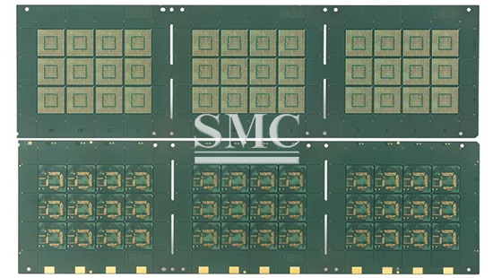
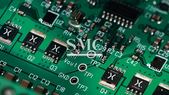
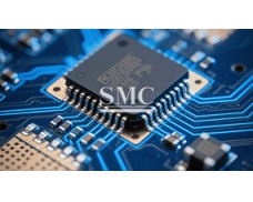
MEMS Sensor IC Package Substrate is a packaging carrier for mounting MEMS chips, mainly including organic substrates, HTCC, LTCC and DPC ceramic substrates. Substrates of different materials adapt to various operating conditions, and are widely used in devices such as accelerometers, gyroscopes, pressure sensors and MEMS microphones for consumer electronics, automotive electronics and industrial measurement‑control equipment. The substrate realizes electrical interconnection and physical mechanical support among chips. By controlling substrate warpage and coordinating thermal‑expansion coefficient matching between substrate and silicon chips, it relieves internal stress generated by thermal cycling and assembly, reduces failures including sensor zero‑point drift and sensitivity shift, guarantees the consistency of signal acquisition and output of MEMS devices under operating conditions, and meets structural and electrical performance requirements for sensor packaging.
If you want to know more about our If you want to know more about our Electrical & Electronics products or MEMS Sensor IC Package Substrate price please feel free to contact us, we will reply you within 24 hours.







|
MEMS Sensor IC Package Substrate |
||
|
|
Parameter |
|
|
1 |
Substrate Type |
Organic BT / HTCC / LTCC / DPC |
|
2 |
CTE |
BT:12-16;96%Al₂O₃:6.5-7.5;AlN:4.5-5.5;LTCC:7-9 |
|
3 |
Thermal Conductivity |
BT:0.3-0.5;96%Al₂O₃:20-30;AlN:170-200;LTCC:2-5 |
|
4 |
Dielectric Constant Dk |
BT:3.8-4.2;LTCC:5-7 |
|
5 |
Dissipation Factor Df |
<0.008 |
|
6 |
Glass Transition Temp (Tg) |
170-220 |
|
7 |
Layer Count |
Organic:2L/4L;HTCC:2-8L;LTCC:2-12L |
|
8 |
Total Substrate Thickness |
Organic:100-250μm;HTCC/DPC:0.25-0.635mm;LTCC:0.2-0.5mm |
|
9 |
Panel Dimension |
180×60;210×250 |
|
10 |
Copper Thickness |
Organic:8-15μm;DPC:10-100μm |
|
11 |
Cavity Depth |
0.1-0.5 |
|
12 |
Trace width / Space (L/S) |
Organic:25/25~35/35μm;LTCC:40-60μm;HTCC:≥80μm |
|
13 |
Blind Via Diameter |
65-80 |
|
14 |
Landing Pad Size |
120-130 |
|
15 |
Registration Accuracy |
Organic:±15;LTCC:±20;HTCC:±30 |
|
16 |
Surface Finish Type |
Ni/Au、ENEPIG、OSP、Ag |
|
17 |
Ni Plating Thickness |
2-5 |
|
18 |
Au Plating Thickness |
0.05-0.3 |
|
19 |
Warpage |
Organic:≤0.3-0.5%;Ceramic:≤0.2% |
|
20 |
Operating Temperature Range |
Organic:-40~+125;Ceramic:-55~+150 |
|
21 |
Pad Pitch |
0.4 / 0.5 / 0.65 / 0.8 |
|
22 |
Compatible Package Type |
LGA / QFN / LCC |
|
23 |
Wire-bond Compatibility |
Gold wire bond applicable |
Standard Packaging
MEMS Sensor IC Package Substrates are precision micro‑electronic components sensitive to mechanical shock, static electricity, moisture and warpage. For export shipment, substrates on production panels are first separated or kept in original panel format according to customer requirements. Each panel or singulated unit is placed into anti‑static moisture‑proof tray or antistatic carrier tape with protective cover film to avoid scratching circuit surfaces and solder pads. Desiccant and humidity indicator cards are added inside moisture‑proof aluminum foil bags, which are vacuum‑sealed to control internal humidity and prevent moisture‑induced delamination or oxidation. Sealed bags are packed into rigid ESD‑shielded inner cartons with foam cushioning for shock absorption. Multiple inner cartons are consolidated into export‑grade outer cartons reinforced with corner protectors. Outer cartons are marked with labels including ESD warning, moisture‑sensitive device mark, part number, quantity, destination information and shipping marks. All packaging complies with international export logistics requirements to protect substrates against vibration, impact, static discharge and humidity variation during long‑distance sea or air transportation.
Shipping
We support FCL and LCL sea freight, air freight and express delivery, subject to order quantity and destination country. Trade terms include EXW, FOB, CIF. Other terms may be available upon request. Shipping costs are calculated based on cargo volume, gross weight, destination and selected transportation method.
Lead Time
Samples: 7-10 working days
Standard orders: 30-35 working days
Customized order: 30‑35 working days


Q1:What is the main difference between organic and ceramic MEMS sensor IC package substrates?
A: Organic BT substrates feature lower cost, finer trace capability and thinner thickness, mainly for mass‑production consumer MEMS devices. Ceramic substrates (HTCC/LTCC/DPC) have better thermal stability, matched CTE and optional hermetic cavity structure, targeting high‑reliability scenarios. Ceramic substrates generally cost higher than organic counterparts.
Q2:Why is warpage a critical indicator for MEMS package substrates?
A: Excessive substrate warpage will introduce extra mechanical stress onto MEMS sensitive chips and diaphragms. It causes zero‑point drift and sensitivity shift of accelerometers, gyroscopes or MEMS microphones, and may also lead to poor wire‑bonding contact during assembly.
Q3:What surface finish options are available for MEMS sensor IC package substrates?
A: Common surface finishes include electroplated Ni/Au, ENEPIG, OSP and silver plating. Ni/Au and ENEPIG are widely adopted for gold wire bonding. OSP is cost‑effective for non‑wire‑bond mass‑production products, while silver is mostly used for LTCC substrates.
Q4:For automotive‑grade inertial MEMS (accelerometer & gyroscope), which substrate material is preferred and what key parameters shall be controlled?
A: HTCC 96%Al₂O₃ or AlN substrate is recommended. Key controlled parameters: CTE matching with silicon die, warpage ≤0.2%, operating temperature range ‑55℃~+150℃, qualified Ni/Au plating for wire‑bonding, and helium leak rate for hermetic packaging. Poor CTE matching will trigger obvious zero‑point drift under temperature cycling for inertial sensors.
Q5:What challenges will LTCC substrates face when applied to MEMS microphones?
A: LTCC can integrate acoustic cavity conveniently, yet it has limitations. Higher dimensional tolerance is required for cavity depth; improper residual stress during sintering brings warpage risk. Its thermal conductivity is low, and line‑width performance is inferior to organic BT substrates. Registration accuracy and cavity dimensional consistency need strict process control for mass production.
Q6:What risks may occur if using standard IC organic substrates directly for MEMS sensor packaging?
A: General IC substrates do not optimize CTE and warpage for MEMS sensitive structures. Under temperature cycling, unmatched CTE and excessive warpage generate stress on MEMS diaphragms, resulting in zero‑point drift, sensitivity deviation or even mechanical failure. Standard IC substrates also lack targeted stress‑release design for MEMS‑ASIC co‑packaging.
here
for
price